How Raspberry Pi built a silicon design team | #MagPiMonday
This #MagPiMonday, we meet Raspberry Pi’s ASIC design team to talk about chip design.
Alongside building single-board computers and microcontroller boards, Raspberry Pi is heavily involved in silicon design. For nearly ten years now Raspberry Pi has been building an ASIC (application-specific integrated circuit) team in Cambridge to design and produce custom silicon chips for its products

This intricate process involves designing integrated circuits on a silicon wafer. We sat down with Tammy Julyan, ASIC Engineering Director and Nick Francis, ASIC Technical Director to chat about Raspberry Pi’s ASIC team, and how they go about designing silicon chips. It’s a fascinating deep dive into bare metal computing.
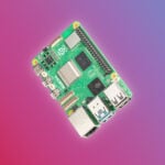
Raspberry Pi makes computers using components like the Broadcom BCM2712 System-on-Chip, Renesas DA9091 power management unit, and Infineon CYW43455 Bluetooth and Wi-Fi chip.
However, for the last 10 years Raspberry Pi has also been designing its own chips, such as the RP2040 microcontroller found in Raspberry Pi Pico and the RP1 I/O controller found in Raspberry Pi 5. These contain smaller blocks, often referred to as IP (intellectual property) designed by Raspberry Pi or bought in from elsewhere and integrated into Raspberry Pi’s chips.
Integrated circuits
Silicon is basically sand, which is the world’s most abundant element after oxygen. Silicon is a semiconductor, which means it can conduct electricity under some conditions but not others, making it ideal for controlling electrical current. It is turned into silicon wafers, which have patterns etched onto them to create integrated circuits.
An integrated circuit (IC) also known as a silicon chip, microchip, microelectronic circuit or computer chip, is an integrated system of multiple miniaturised and interconnected components embedded into a thin substrate of semiconductor material. ICs are made up of millions of tiny transistors. They have many different functions, and can be found in products ranging from automotive, computing, and medical equipment.
Tammy Julyan has worked with Raspberry Pi for nine years and is responsible for the tiny Raspberry Pi logo on the silicon
Nick Francis has been with Raspberry Pi for seven years and has worked on RP1 and RP-2040
Silicon design is specifying, designing and testing an IC. It also involves creating the physical layout of the chips’ circuits. This consists of a team of skilled engineers working together using their expertise to ensure the final design meets the original requirements.
The first step is the specification. Requirements can come from several sources, an innovative new idea, customers, internal product needs, and marketing forecasts. For example: RP1 was designed to hang off the main processor as a southbridge, handling most input and output capabilities for Raspberry Pi 5. It controls the camera, display, Ethernet, USB, and GPIO.
“We start with a team of people from across the different groups including software, hardware and management to discuss a new chip: ‘let’s make X to do Y’,” says Tammy. Architecting a new chip is an iterative process, and the whole team will meet multiple times to discuss what the “shape and feel of the thing” needs to be. Many factors are considered: performance, timescales, make vs. buy, interfaces, features, power, board-level design, and software.

Most devices are system-on-chips (SoCs), they have a controlling processor, some memory, and some peripherals which perform functions such as data processing or an interface to the rest of the system. “You need to consider how these blocks communicate with each other and what software will run to control the system. The ASIC team also needs to consider a whole host of other things like how to start up the device, what clocks are running, how to cross clock domains. There’s a very long list. So now you have an architecture and can start to build your chip.”
Some of the blocks Raspberry Pi may already own, and can be reused from a previous design, while some the design team needs to build from scratch or buy. However buying in a block – or IP – isn’t an easy process: they need to choose the right vendor, configure the block correctly, integrate and verify it.
“Chip design is written in a language called Verilog” explains Nick. It is a bit like C but “it doesn’t execute in order; it executes all at once”. Verilog is a hardware description language (HDL), that describes in code how the circuit functions.
Testing the design
Once the design is complete you have to test that it works as expected before it is committed to manufacture, this activity is known as verification. Verification is a huge part of the silicon design process: “I think the biggest difference is that software – even if it’s well tested – can be more easily changed afterwards,” says Nick. So “most of my time is spent testing”.
Software code, either C or Verilog, is written to stimulate the design and the output is checked. This testing can be at the block or chip level, normally done through simulation.
Some block or chip-level testing uses constrained random techniques to generate test conditions that are hard to predict. “We can run many of these random tests to help find corner case issues.”
As well as simulation tools, FPGAs (field programmable gate arrays) are used to test the design. An FPGA is physical hardware that can be reconfigured to emulate different hardware circuits, this enables testing to take place in near-real-time in hardware (instead of being simulated in software, which is much slower, being limited by available processing power). FPGAs are useful for system integration testing and software development before the chip is available.
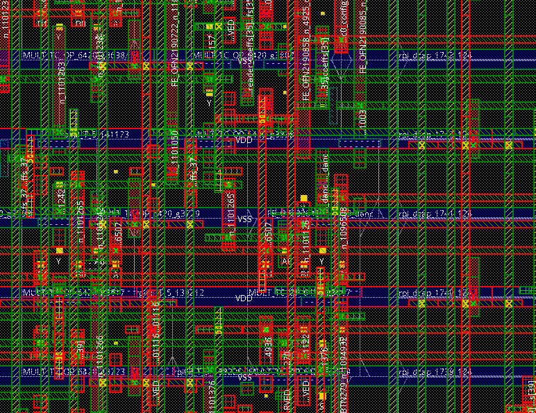
Once the design is functioning as expected, the HDL needs to be converted into a physical design which is a representation of the geometric shapes that will create the tiny transistors and connections on the final chip.
Extra functionality is added to the design to support manufacturing tests to check for defects that could affect the correct operation of the IC. Some of these extra Design For Test (DFT) functions are structural and are inserted using tools which also generate test patterns to test logic cells, and some are internal Built In Self Test (BIST) engines to test things like memory. To convert the HDL, it is loaded into a synthesis tool along with a timing constraints file called SDC (standard design constraints) and libraries: for example, logic gates, memories and analogue blocks. The synthesis tool converts the Verilog into a gate-level netlist which is functionally equivalent to the HDL description, making architectural decisions based on how fast the design needs to run, while also considering the power and area to get the most optimal design.
After synthesis, the gate-level Verilog netlist is loaded into a ‘place and route’ tool where a floorplan is created, positioning the memories, analogue blocks and any IO. A metal power grid is added to feed the gates with power across the floorplan. The standard cells are then placed in rows by the place and route tools, the metal wires connecting up the standard cells, memories, etc are routed. The tool continuously checks timing and when possible fixes any slow paths. The physical design is checked to make sure it is functionally correct, meets the timing requirements and can be manufactured correctly. When complete this is sent to the wafer foundry to be manufactured.
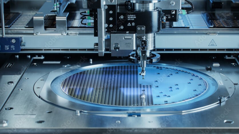
The “manufacturing process itself is interesting,” says Tammy. The physical design is translated into a set of masks, the number of which increases as technology advances. They grow the silicon crystal by dipping a ‘seed crystal’ into molten silicon until it turns into a large cylindrical ingot. Then they are sliced thinly into wafers, ground and polished. Once the wafers are created they go through multiple process steps to create the IC. Photolithography is used to transfer the geometric patterns from the mask onto a photosensitive layer applied to the wafer, and in addition to oxide growth, etching, deposition, ion implantation and metalisation the IC is created. When complete, the wafer is covered in rows of ICs which need to be divided up into individual chips by sawing and placed in their packages. Once packaged they are tested to ensure nothing has gone wrong in the manufacturing process.
Ten years ago Raspberry Pi had no ASIC design capability, and since then it has developed from the ground a highly talented design team. We look forward to seeing what they create next.
The MagPi #142 out NOW!
You can grab the brand-new issue right now from Tesco, Sainsbury’s, Asda, WHSmith, and other newsagents, including the Raspberry Pi Store in Cambridge. It’s also available at our online store which ships around the world. You can also get it via our app on Android or iOS.
You can also subscribe to the print version of The MagPi. Not only do we deliver it globally, but people who sign up to the six- or twelve-month print subscription get a FREE Raspberry Pi Pico W!


4 comments
HankB
From Wikipedia.
“Sand is primarily made of silica, which is silicon dioxide in the form of quartz.”
(Resident Pedant.)
Cary D
Given Raspberry Pi’s programming heritage, I can’t understand why the chip numbering didn’t begin with 0, not a 1. So was there ever an RP0 chip, or was this some kind of prototype that never saw the light of day?
xeny
When I did my CS Masters, there was an ongoing battle between academics and admin staff about how things were numbered. You could walk around the department, and see where one side or the other had won the most recent decision, and periodically things would change – I seem to remember at one points lockers were numbered starting from zero, and then next year starting from one.
Duncan
0 is for the IT people.
1 is for admin people.
It depends on who are the majority users.
Software version is 0.1, 0.2, 0.3…
TV drama series is 1, 2, 3… Can it start with 0 :-))
Comments are closed