High-res pics of the PCBs
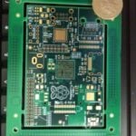
Many people (I was one of them) found last week’s printed circuit board (PCB) pictures a little hard to decipher, because they were teeny-tiny and taken with a camera phone. Pete’s sent me an unpopulated board, which I’ve just been photographing with a proper camera in the six minutes of winter sunshine we get every day in Cambridge. Here are some much more detailed pictures which you can click on to enlarge so all the silkscreening and visible tracking can be seen.

Raspberry Pi unpopulated PCB, front. Click to enlarge.

Raspberry Pi unpopulated board, back. Click to enlarge.
I should make a couple of points here to clarify what you’ll get when you order your own Raspberry Pi. We show you pictures like this and explain where we are in development and manufacture because we’re very interested in providing transparency about the way we work, especially because we have such a large and information-hungry community. Unfortunately, some people who aren’t used to this approach do sometimes jump to conclusions about what we’re doing as a result. So:
You will not be sent a bare board like this that you have to solder parts onto yourself. This is just an illustration of what the boards look like part-way through the manufacturing process. We’ve been a little surprised that our decision last week to show you the boards before they’ve been finished led immediately to speculation in some quarters that we weren’t going to bother doing all the work to populate them. Please don’t worry: there is absolutely no soldering required in the finished product. There’s a lot of fine-pitch BGA mounting on this board (which you’ll see if you click through to the larger pictures), and this is impossible to solder by hand; it’s why we use robots. Some of the components, specifically the very large bits like the connectors, are soldered by hand in the factory, because this works out a little cheaper than using robotics, but the vast majority of the parts are mounted by pick-and-place robots, and we can’t sell them to you separately.
After all that, though, I should point out that we are not shipping with the GPIO pins connected; those who want to use them have asked us not to because they want the flexibility to mount them to project from the front or the back, and some want pins with a 90º bend for their own projects. If you’re planning on using the GPIO, you’re already a hardware hacker with a good idea of how to mount them, so we’re not concerned about this.
The mounting you see around the edge of the board will not be there when you buy your Raspberry Pi, and we can’t make a separate batch with it still on as some have requested; it’s there for manufacturing purposes only. Some people also suggested we were wasting copper when they looked at the mounting because they could see the little squares embedded in the frame. This is actually an artefact of the PCB making process: without those squares, the flow of substrate at the edges of the board is unpredictable and can be too thin to support the layers of circuit board. Those squares ensure that the flow is even all the way up to the edge. We are signed up to a whole host of electronics waste management agreements, and I promise you that we do our very best not to waste anything. Quite apart from worries about the environment, it wouldn’t be a cost-effective way to work, and we are really very serious about bringing the Raspberry Pi to you at the very low prices we’ve been promising all along!


182 comments
walney
OOH! Nice (and first post) – preserving a long tradition of adding nothing to a discussion :)
Fabio Grande
I just can’t wait to see pictures of a POPULATED Raspberry…. ;-)
Thunder__X
Huzzah!
Bizzo
Well it looks like you’ve thought of everything, dotting the i’s and crossing the t’s so to speak. Except there is no dot above the i in the logo on the board.
Will you be supplying some boards with the i’s dotted? :-)
liz
I know you’re not being entirely serious here, but it’s an interesting point – as it happens, it’s very hard to reliably silkscreen dots at this sort of size, so we avoid them.
Bizzo
Sorry, yes, I wasn’t being serious at all, but thanks for the explanation.
If I really wanted a dot, I’m sure I could do it myself with a bottle of tippex and a fine brush.
WASD
You may want it to say uppercase PI then. Looks like P1 now.
WASD
Or Pi with another font.
ProDigit
The next board will have P2 (spell Pee too) :-)
Sam Swain
To those concerned about a few squares of ‘wasted’ copper, can I explain that PCB manufacture is a subtractive process, that is; the board layers start fully covered in copper and then removed by chemical etching. So, the more you leave on the board the less there is left in solution in the etchant (that has to be disposed of or reclaimed). This (and many other techical reasons) explains some odd shaped/patterened areas on a lot of PCBs you may see. Other reasons include: screening, preventing rippling of the protective coating, ensuring solid mask printing, reduced copper waste, not to mention all of the circuit constructs that you find on some specialist boards (e.g. antenna, track length balancing, logos, etc).
liz
Thanks Sam! A lot of the manufacturing process is new to me, too; and it’s much more interesting that I’d anticipated.
kkolev
Is what we see on the south side of the main chip (just above L1, L2, R14) track length balancing?
ds
Sure looks that way. Those traces are going to the HDMI port, which is a high speed connector. The higher the speed of the signals being transmitted on a pair of wires, the more important it becomes to balance them so your signals arrive as close as possible to each other at the destination. If you don’t balance the signals, you have to slow down your transmission speed to get reliable behaviour.
ProDigit
First thing that came to my mind Sam, however, it is possible to equip the board with less copper as they make them, but I don’t see if it would save a penny in manufacturing!
Sam Swain
I’m afraid that the economies of scale that apply in mass electronics manufacture make that very very unlikely. …until one day when we have machines that just ‘print’ the copper directly onto the substrate. :O)
Greg Smith
For boards with very thin traces, there is also an additive technique: start with a very thin layer of copper, apply mask where you don’t want copper, then electroplate copper up to proper thickness. Then, remove mask and etch the whole board enough to clear the areas which were masked. This avoids undercutting thin traces, and is generally done only on outer layers where you need thicker copper. The rate of electroplating in a given area depends on current density in the plating tank, which depends on the average density of copper in that general area, so it’s common to fill empty areas with copper dots (or make small holes in large ground planes ) to control this. In any case, all the waste copper, whether it’s in a removed border, or in chemical etchant, can be recycled, and there’s no cost to the customer for extra copper dots. Cost is generally based on area (obviously), number of layers, difficulty (fine lines, etc), special features like selective gold plating or screened-on resistors, and the number of holes to be drilled.
psergiu
Thanks for the Hi-Res pictures.
Now we want the pictures of the robots mentioned in the post :)
PS: can someone detail what connectors will NOT be soldered on the final board ? (GPIO …)
liz
Good point – it’s just the GPIOs, but I’ll add that to the main post.
psergiu
Thanks !
What about the Camera (CSI) & LCD (DSI) connectors (S2 & S5 on the front of the board) ?
jamesh
I posted this in another thread the other day, but of interest here.
I was in the pub on Saturday and the landlord has a Pick and place robot for sale. I jest not. It’s a Samsung, and you can have it for £25k. It does about 3600 components/hour.
He could also sell me a brand new model (Samsung again), which could do 18k components per hour. That was £90-100kish. This is a twin gantry 6 head machine capable of the placing the smallest components available (you know, the resistors that look like dust particles).
Quite an interesting chat.
liz
The pub landlord? There’s diversification for you.
I suppose we know where to go shopping if we decide to vertically integrate!
Michael
> the landlord
Only in Cambridge!
Sancho
Don’t take me too seriously.
You rule at device creation.
You suck at taking a simple picture of it :)
Anyhow, thanks – still far better than the low-res.
Can’t wait for the device – any update on the schedule? E.g. expected week or such?
liz
It all depends on testing.
JaffaBoy
Many thanks for the updates Liz, just a shame that some poeple jump to conclusions rather than ask a simple question.
Cannot believe that some people would think you’d be supplying an unpopoluated board, because, that would really help get more kids get into programming wouldnt it ;-)
I hope it doesn’t put you off giving out information in this way, it certainly helps mellow the wait for the final product.
pauldow
This blog post did have me realizing that keeping things secret Is so much easier than explaining everything. That was uncomfortable to read, knowing some of the thought process needed to write it, based on past messages from the public here.
That said, I’m curious about some traces on the front of the board. (This is not a complaint!)
Below the big Broadcom brains of the Pi are 7 pairs of traces, most running diagonal to the lower-right. On most of the pairs, one of the lines runs zig-zag for a bit. I was wondering what that does. I rarely look too closely at PCBs too closely, but sometimes the art that goes into them is interesting, such as high frequency RF electronic equipment design.
pauldow
oops, I guess I don’t read what I write too closely either.
pauldow
Never mind. I went over to the forum, and it’s already been asked, and answered.
http://www.raspberrypi.org/forum?mingleforumaction=viewtopic&t=1436
daveg
Looking good.
Pete and his company are professional PCB manufacturers not a bloke in his garage with a bottle of ferric chloride from maplin and a converted fish tank. The board is designed and manufactured the way it is for reasons that most of us will never comprehend. Let the professionals do their work and don’t try to second guess processes we don’t know about. Just be grateful they are showing us the progress
Jongoleur
Oh! The simple pleasures of single-sided board creation!
I did it using an old photographic paper tray – in many ways the process was just like development by inspection!
mdf200
Any chance of buying bare boards? I quite fancy mounting a couple in a frame! :)
liz
We’ll have some boards which we’d otherwise have to throw out because they’ll have manufacturing errors in them (those of you who work with PCBs will recognise this as an inevitability), and we’re planning to sell them so people can use them as coasters, frame them, stick them inside plexiglass or do whatever they fancy with them – on the understanding that they won’t work!
walney
Sign them first!
Ken Pemberton
^^^ what he said
mdf200
Oooo.. Yes please! I’d pay normal price for them as well!! :)
Ken Pemberton
me please!
Adrian
Oooo!! Put me on that list. I would love to get my hands on one, my own little piece of history. Signed would be great!!!Can’t wait to see pictures of the populated boards. You are doing a wonderful job, keep the info coming.
Guy
Framing them! Bah! FFS!
Populate the board and give it to some kids to play with. Are you the type of person that collects the chewed gum of hollywood stars?!
jamesh
Yes.
Neon22
yes here is my collection:
http://www.moulicohen.com/2010/09/03/replacing-plastic-with-recycled-chewing-gum/
DeliciousRaspberryCake
Very delicious circuit board for a very delicious Raspberry Pi computer
Is there a place I can drill a mounting hole in model B? Will the ethernet connection spot be available to put a screw through on revision A?
Also, I’d hate to be the person having to mount the larger components onto the board by hand, it must be extremely tedious work as even the “largest” component on this board is only 1cm big (ethernet and usb block).
John Sanderson
Don’t even think of drilling holes! Two reasons, first you could end up shorting the earth and power planes together, secondly you don’t know where all the tracks on the inner four layers go and could drill through a dozen tracks easily!
axiomprime
I am now at fever pitch.
Montekuri
Don’t take my words too much serious :D
Someone will still complain that the pictures were not taken from just above the board (90 degrees)
liz
Yeah – I know, but there were problems with shadows doing that. I don’t think anyone’s really too bummed out about it.
psergiu
If you place the board on a flatbed scanner – will the images be better ?
n1ywb
Yes, a flatbed scanner would work beautifully. In fact it might even be TOO good, you’ll be able to see EVERYTHING ;)
Jan
Yes, indeed. I learned it’s the preferred method for CPU collector photos, then you have all the text and other bits perfectly sharp. Alternative would be “tele macro” which keeps the edges too sharp but you need good stable setup and more light than usual. Anyway for this kind of board, it’s good enough even if a little blurry.
cougarten
http://img6.imagebanana.com/img/rnrbxkjm/front.jpg
http://img6.imagebanana.com/img/0kiuz2nd/back.jpg
still a little distorted, but should do the trick for most purposes
Paul Morriss
This whole process is not just an education on how to work with embedded computers, it’s also an education on how modern stuff is made. I used to work for a firm that designed and programmed boards like this, so I know some of it already. It’s still exciting though!
ejamie
Completely agree. The ability for the average small shop to effectively mass-produce reliably has enormous potential, and I think we are only at the beginning of this trend. For example, see maker bots. Think how the printing press revolutionized books and society… now, imagine the same concept for any/all digital hardware construction. :-)
RPi team, thanks for keeping this as transparent as possible. Any additional sharing or open-sourcing your process documentation could open a new door for the RPi community to contribute to future hardware versions or perhaps build their own re-saleable add-ons.
Method
So these are the final unpopulated boards. It looks great, I love the Pi logo, but one thing that I’d like to ask:
If the device doesn’t come with the mounting edge, will there be no fixing holes on the device itself, for fixing into cases and the like?
liz
We’ll probably be putting out a revision next year some time which does have mounting holes, but I’m afraid that for now, there aren’t any. Sugru (or Blu-Tac for a less permanent solution) is a good way round the problem.
Bob H
I’ve visited the factory my company uses and seen the ladies doing the mind-numbing task of fitting SCART connectors: respect to them. However, the most impressive thing in production is the slightly risky task of machine placing through-hole components with the “shotgun process”, so described because it sounds like a shotgun as it puts a large capacitor into the board. Good thing RPi doesn’t appear to be using large through hole components in this way, it increases the risk of failure during production.
Jan
Yeah, the THT placing is ridiculous, you need to have exactly straight leads in the right pitch the component must be just upright. I can’t find many examples, but here’s one with LEDs only: http://www.youtube.com/watch?v=h4SbJwIjBP4
toadstool
I’m sure it has already been said but may I add my own voice to the chorus; I admire the patience you and your colleagues exhibit. I, for one, would have lost ‘it’ long ago. I hope the detailed post above will quell the tide of inane questions enough to allow your sanity to return. I mean, people could be really dangerous if they searched for answers before asking questions! I propose that the day of release should be known as Saint Elizabeth’s day, if there isn’t already one ;-) Lovely detailed photos by the way.
jamesh
I think the only thing that will quell the tide of inane questions is……….er…….nope, cannot think of anything.
PiOfCube
Absolutely brilliant :-)
I’ll get some 3D models made (components and stuff) and packaged up ASAP. I’ll also create some general purpose video sequences showing different aspects of the board.
I’ll make it so the individual components can be removed/animated in case anyone wants to do a video showing how to hack the board or even to demonstrate how it all works (which is what I’ll be doing).
The only thing is, by adding the artwork onto the models, it might cause copyright issues. I was going to release all the work under the Creative Commons licence but to get around any problems with confusion about whether or not the actual PCB design is Open Source, I think it would be a good idea to make up the models without the texture applied and supply that separately. Then the models (which are just common components and a flat board) can be released under CC without any issues… those wanting to make it look like a R-Pi board just need to apply the texture. I know some might say that the placement of the components would be arranged to fit in with the PCB design so if the Raspberry Pi Foundation has no objections, then I’ll do it as stated. Also, as it will be released under the Creative Commons licence, I won’t be making any money on it and the R-Pi foundation can use them in anything they wish (if they think it’s good enough) ;-)
liz
That’s fine – thanks for checking, though!
High-res pics of the PCBs | Raspberry Pi | Raspberry Pi | Scoop.it
[…] High-res pics of the PCBs | Raspberry Pi High-res pics of the PCBs | Raspberry Pi http://t.co/UziGS58C… Source: http://www.raspberrypi.org […]
Homer Hazel
In the event some bare boards fail QC, I still want to buy one. Also, should one of the assembled units fail QC, I would also like to buy one of those. Even a failed Raspberry Pi will make nice art
Ken Pemberton
me too! me too!
Brian Smith
Thanks for the pics. Surprising number of passives on the board, looks like. 96 caps and 50 resistors. Are those cat hairs? (the joys of taking hi-rez close-ups).
Lyubo
Hi,
Is it only me or there isn’t a big ground plane on the top and bottom layers.
Burngate
Looks like it’s one of the four middle layers. We’ll have to wait for the CT scan
rickyjames
Wow, you guys are running some thin traces in here – and right up to the edge of the board, too. In the GPIO area on the bottom of the board you’ve got three traces running side by side betwen the two rows of holes that are only 0.1 inches apart centerline. Just “above” that there’s two traces between the row of GPIO holes and the very edge of the board, which means you’ve got traces 0.05 inches from the edge. Holy cow.
Speaking of that trace that’s 0.05 inches fron the edge of the board – is that a copper boundary around the board it’s (accidentally?) running into, or is that just a thicker layer of the solder mask green?
I seem to recall someplace that during the 1980s when Apple did the Lisa PC board layout (before the first Mac) they had things so compact (for that time) that they had to go for two traces between 0.1 centerline holes and had resulting quality problems with the boards that contributed to the high price and failure rate of the Lisa.
Of course, that was close to 30 years ago, and PCB layout has certainly progressed since then – as you are demonstrating. Great work here.
Hunter
You may not know the answer to this, but why do some of the traces coming out of the BGA footprint get all squiggly and then straighten out again? For example, look right above L2 on the front side. I’m not aware of an electrical reason for doing that.
liz
Some of the hardware types on the message board answer this and other questions here: http://www.raspberrypi.org/forum?mingleforumaction=viewtopic&t=1436.0#postid-20182
Hunter
Oh awesome, thanks!
Robin Jacobs
This is a bit off-topic, but have you considered adding a Flattr button to the blog posts? :p
Also, will the Raspberry Pi still be released this year, or will it be somewhere in 2012?
OrangeThoughts
“led immediately to speculation in some quarters that we weren’t going to bother doing all the work to populate them”
AHAHAHAHAHAH. HAHAHAHAHAHA. HAAAAAAAAAAHA.
god bless stupid people.
HuiJun
–> You will not be sent a bare board like this that you have to solder parts onto yourself.
That is the worst news yet.
Ken Pemberton
I’m sure if you ask *really* nicely they’ll ship you a bare board for an additional fee ;-)
jamesh
I find it somewhat amusing to keep read these post from people who fancy soldering up the board themselves.
I reckon that about 0.001% of people would be able to put one of these boards together so that it works.
That’s a lot of rotten raspberries and cheesed off raspberriers.
TinWhisker
Challenge accepted…
David Riley
Well. It’s certainly doable, but it’s excruciating. If you’re using a heat gun and not using lead-free solder, surface tension will often pull the BGA into proper position (though with that fine a pitch, it’s way too easy to misregister it by one ball and only find out when you plug it in and it doesn’t work/catches fire). Certainly something I’d *rather* have a robot do, because they do it a lot better. We do have techs where we work that can do it with a better than 50% yield, though, which is at least good for a human.
jamesh
Never said it was impossible, just very very difficult, and not worth the extra $5 it would probably cost to get it in kit form. Even for ‘fun’.
Ken Pemberton
Stop whetting my appetite and start shipping already! My wife keeps asking me what I want for Christmas…
greg jaskiewicz
So will the next one be called Rasbery P2 ???? ;)
I’m referring the font on the board. “Pi”, where the letter ‘i’ looks like subscript :)
Richard
Excellent pics! Can’t wait to get my hands on these!
I’d like to say, tho, that it always disappoints me that the blog posts have to address community speculation; like these boards not coming populated. I think *anyone* who’s spent more than 5 minutes following RasPi should totally know they’re getting a complete, fully functioning, modern, compact and capable ARM personal computer!
Come on guys, *read* before you speculate! I’m sure it only annoys them over at Raspberry Towers :)
Jessie
Thanks for the update. I would think it would save you a lot of headache just to not post things, I just don’t understand how easily confused people are. Back in the day I thought I wanted to be an artist, I got to my internship and when I had to deal with ignorant customers I changed majors and restarted. I can’t tell you how many people just wanted to pay an artist to make steaming piles of crap for them. Or how many times people would ask to see a work in progress and they exclaim that it looked like shit. Really it looks like shit? That is because it is about 10% done, this isn’t Star Treak we don’t just say: “Computer make me something cool” and bam its done. I eventually got an IT degree, but ended up becoming an industrial electrician / welder just to avoid interfacing with customers.
axiomprime
Rudeness often flows with money. Bosses and customers can talk to you in ways that most other folks can’t.
Fabian
Thanks for sharing! Can’t wait for the final board :-)
Matthew
Could the solder mask be changed from green to red without increasing cost? Red seems more akin to raspberries!
manuel
Thats a good idea!
liz
Unfortunately, it’s more expensive. We did look into it; we might do limited edition runs in red later on, but that’s for the future.
Ken Pemberton
Put me down for one of those! *THAT* one goes in a perspex housing, I think… or maybe (just for the fun of it) a glass one. Oooh I just got an idea!
David Riley
Usually it does; it’s a volume thing (green is the most common, so it’s cheapest, just like DDR3 is cheaper than DDR2 now even though it’s much faster). In my experience, it’s only a few percent difference, but if it would force them to divide up their manufacturing run to provide different colors, that would drive up the cost quite a bit.
For the boards I’ve made, it only costs about 20% more (for the lot, not per board) to make 1000 boards instead of 100 (and the scales follow similarly up). When you divide the number of boards you produce at a time in half, you nearly effectively double the per-board price because most of the cost is in the tooling and setup. So if it cost £85 to make 50 boards and £100 to make 100 boards, making two lots of 50 boards (for two different colors) would cost £170.
At work, we tend to make our prototype boards green (often because the prototype PCB houses only do green for their cheaper specs) and do the production board in colors so that we can easily differentiate them in the field (and it’s cheaper to do the color once you’re doing it in real volume).
Ken
Hey Liz,
sorry if this question has been asked before, but how thick is the pcb itself? i can upload a model of a mount for everyone on shapeways.com and it would kind of alleviate some of the issues of not having mounting holes, for those who need them.
Best Regards, Ken
liz
It’s barely over a mm – I don’t have anything finer pitch to measure it against than a ruler marked in mm, but I’d estimate it to be about 1.1-1.2mm.
walney
Liz,
I’ve got some vernier calipers, so if you’d like to send me a board I can accurately measure it for you!
Ken Pemberton
LOL @ walney!
I’ve got a computer-assisted, laser-guided, nanometer-rater gauge…
:-)
walney
I don’t even know what one of those is… :-(
quired
You should really use a micrometer for this sort of measurement.
TMR
I think ordinary verniers should do the trick– a good snap fit is probably attainable with even tenth-of-a-millimeter precision.
Greg Smith
So stack up 20, measure, divide by 20
liz
That would have been my first impulse, if there happened to be more than one of the things in the county. Sheesh.
Roger Wolff
Liz, standard PCB thickness is 1.6 or 1.4mm, although nowadays other thicknesses are available as well.
Anyway… Maybe things are a bit different for the 4+ layer boards. This is a 4 layer board, right? 6?
liz
Six. ;)
aygun
As far as I know , I will not need the GPIO connector.
Al what we wanna do is an router with some extra things .
Me and the developer of webhtb will use this boards to make some routers with this microcomputers .
We are wainting the date when yu guys will sell this toys.
Keep up the good work !
Raspberry Pi Platinen | Loco Toys Blog
[…] Hier kann man die Platinen in hochauflösenden Bildern bewundern… Habe ich schon erwähnt, dass ich dringend einen (oder 2 oder so) von denen möchte? Dieser Eintrag wurde veröffentlicht in Computer und verschlagwortet mit Raspbery Pi, SoC von Florian Heer. Permanenter Link zum Eintrag. […]
polyhedra
nice if it have and explorer for the internet, i can surf and find origami diagrams. and write code if BBedit works :P
Robert_M
“Mr. DeMille, I’m ready for my close-up!”
Or, in the words of Billy Crystal:
“You look mahhhhvolous!”
polyglot
Nice layout skills; I’ve never done anything past 50MHz. Looks like that board has copped a nasty impact though, there’s starring of the fibreglass between R47 and C95 (right hand side of back.jpg).
I’m all in for one as a media server (mpd, mplayer, etc; maybe xbmc or mythtv) but I’m a little disturbed by the lack of mounting holes – all I need is a 3mm in two opposite corners with a couple mm clear space around that for the standoffs. Chunks of putty or stick-on rubber feet are not a professional PCB mounting method and there doesn’t seem to be enough clearance between the components and board edges to put the board into slots.
Ken
the holes on this mount are .125 inch ~ 3.175 mm
http://www.shapeways.com/shops/nd
polyglot
As per other replies by liz, you don’t get that surrounding thing – it’s used I think as a grip for the pick and place robot and then machined off once the board is loaded. The actual rpi has no mounting holes and they suggest sugru (!) for mounting.
Kevin Vermeer
This is an alternative to the surrounding thing. It’s a plastic part which clips on to the edge of the PCB and provides mounting holes. You’d probably want to glue it on for extra strength, but it would provide consistently located 1/8″ holes with which to mount the board.
Scott Bridges
This mount looks like it should work well. If you order, you might want to order two or three(if you think you’ll need them) as the shipping for a single is $6.50 to the US. I assume they can put three in the same envelope for the same $6.50. The design looks nice though. Have these been tested with a protoboard? Will they be available to order as soon as the RPi is? I’m trying to think ‘gift package’.
Greg Smith
It can be properly mounted by enclosing – ideally in a small plastic box, but another approach would be two nylon tie wraps, hopefully bearing on the larger connectors. I agree that even some very small mounting holes would be nice. But I don’t see room for them…
peter green
Another mounting option that is likely to work pretty well and look pretty proffessional would be to mount the board on top of another PCB using the GPIO and JTAG headers.
This is probablly only worthwhile if you actually want to use the GPIO for something though.
Reuben Sumner
A better way to take pictures of something like this is to scan it in a flatbed scanner.
Michael
It is possible to get somewhere the board’s shematics ? (Don’t worry, not to make any copy , but to develop some hardware)
Awsome work !! Will buy some when it come out !!
Burngate
I was just having another gaze at these (some people go to art galleries for this …) and noticed that not only are a lot of the through-holes filled with copper (middle layers I suppose), but one in particular doesn’t go all the way through – centre-left on the front labeled FD6 is just not there on the back! Yet one more thing I’m too ignorant to understand!
Burngate
I knew it was there: just couldn’t find it.
Now I have.
http://www.raspberrypi.org/forum?mingleforumaction=viewtopic&t=1436.1
Greg Smith
FD6 is not a hole, it’s a plated metal circle called a ‘fiducial’. The pick & place machine has a camera, and is programmed with the positions of the fiducials. It locates the fiducials in the image captured by the camera, calculates the center of the circle, and uses this to fix the exact position of the board — to be more specific, the exact position of the board’s top copper layer — so as to accurately place components relative to their mounting pads. Thus, the placement of the boards in the pick-and-place machine does not need to be super accurate.
Michael Nixon
Excellent work. I can’t wait to get my hands on some Raspberry Pi. I have many ideas for this – I want to get FreePascal working on it (it can target ARM so this shouldn’t be difficult). I will be working on getting openGL class units ported/working for FPC, then porting my game library to it :) Really want one.
Nicolas
Really cool :) Just a question: where can you order one when they will be populated??
jamesh
From this site, hopefully very very early next year.
Nicolas
Thank you Jamesh
DJ
Will it be possible to get boards that do *not* have the through-hole parts/connectors on them? I.e. no power, ethernet, usb, etc? That would give us the option of either attaching the connector (easy :) or using the holes to “mount” the Pi on a carrier board and place those connectors on the carrier. I had to do this with a previous project, and desoldering the RJ45 was a nightmare. Also, leaving the RJ45 off gives two more unplated mounting holes :-)
liz
Afraid not – we can’t afford to add or remove steps from the manufacturing process for a subset of a batch because it all adds cost. (I know that sounds a bit counterintuitive, but that’s the way it is.)
hamjudo
Umm, I may be confused, but won’t the model A ship without the ethernet hardware? If I understand things correctly, the model A is an upgrade over the model B in a few ways. The USB connector assembly is thinner, (although it does mean one less connector). Memory diagnostics run twice as fast. Instead of the bulky RJ45 connector, there are two sleek mounting holes. Without the network chip, power consumption is probably less, although, it may not be enough less to measure.
It most likely that the only reason the model A costs $10 less is do to a pricing error.
Katawa
“Memory diagnostics run twice as fast.”
Because it has half the memory?
jamesh
Yes, no RJ45 on the model A. Half the memory, no LAN chip. That $10 is basically the cost of the components , plus a bit of manufacturing.
Montekuri
Model A has 128Mb of Ram. Model B – 256Mb;
Model A has one USB port. Model B has 2;
Model A has no internet port and no internet chip (this chip can be the expensive part).
hamjudo
The complete list:
Model A has 128Mb of Ram. Model B – 256Mb;
Model A has one USB port. Model B has 2;
Model A has no ethernet or related parts, Model B has 1 connector;
Model A has 2 mounting holes, Model B has 0;
JustACat
Pretty!
Norbini
Maybe it’s the excitement, but the area where the CPU goes (BGA?) reminds me vaguely of the BBC Micro Owl (http://en.wikipedia.org/wiki/File:BBC_owl.svg), i.e. a semi-populated array of dots…
Yup, it’s just the excitement.
Looking forward to getting my hands on the real thing. Keep up the good work!
Rob
Looks absolutely beautiful, how many lovely layers are there?
jamesh
Six.
Petr
I’m sorry that you will not send bare board like this and parts separate. If it would be cheaper or sooner I would try to solder it by myself :).
jamesh
Well, not cheraper or sooner, and almost impossible to solder by hand.
See this thread which has some pictures to give you some idea of the soldering issue…
http://www.raspberrypi.org/forum?mingleforumaction=viewtopic&t=1436
geeus
I would be well up for some hob top solder reflow action.
only really works for reclaiming components but there are plenty of reflow toaster oven tutorials out there.
could be a challange.
I fairness the only component that i can see that would fail hand soldering is the SoC. once that is in place the rest is is possible.
Just finally to say that I am also well aware that the raspi will never be offered in this sort of kit form, I just fancy the challenge
jamesh
Are you aware how small some of the other components are? I’m looking at an alpha board right now and some of the caps are so small you can hardly see them! Just measured one at <1mm long.
Solder those at your peril.
Petr
Let’s make a deal. You send me PCB and components and if I solder it, I get another Raspberry Pi free :).
jamesh
I couldn’t possibly condone gambling, but if you did manage to solder one together, would it work? I reckon the masks and tools you would need to make one by hand would actually cost more than the Pi itself, so not really a cost effect use of your time.
Petr
You are right. It wouldn’t work. I don’t have firmware and I don’t know if I could load it into the CPU. I’m glad for this project and I hope that I will get one Raspberry Pi for my birthday.
jamesh
ONnce made, you can get all the software easily – just off the Raspi website. I would be more worried that you soldered it together incorrectly given how monstrously difficult it would be to do it!
Jancis
guys, get this rollin a bit sooner :) cannot wait, i’m checking this site daily in anticipation for it to be finally released or at least for some interesting news on this topic :)
jean
You can suscribe to rss feed if You want to :)
Eric
Hi, I was looking at the hi-res top picture and noticed the squiggly line traces coming from several pins on IC2. Is the purpose of that to cut down on interference on those signals or something else?
Tozzi
I think the board has just been damaged :(
dustin
They are intentional and needed to manage the timing of the signals on the wires. Yes, adding just that little bit of distance makes a difference!
Eric
I believe it. I’d really love to hear a talk on how one arrives at the right “squiggles” if you will, to handle timing issues.
Chris de Bruin
I have to admit that in 120 replies I’m shocked not to see a reference to the original great cheap British computer! Even a Yank like me remembers Sir Clive Sinclair’s ZX80 and ZX81 and just like Liz mentioned, those came as a bare PCB and you had to solder all the components to it. Maybe I’m just too old :D
Of course back in 1980-81 those PCs were $99 USD and the R-Pi is only 1/4 of the price with so much more hardware and expansion capacity. 700Mhz vs 1Mhz how fare we’ve come :D
axiomprime
The guy that made the BBC, Chris Curry, used to work for Clive. It’s one of his company’s offshoots that designed the chip in the Pi. If you adjust the price of the ZX80 for inflation, it’s almost 400quid. We have come very far.
Chris de Bruin
Very cool. Thanks for the trivia update. I loved my ZX81 back when I was young, its very cool that I’ll have a spiritual successor back in my home :)
sharparrow
Those pictures are much better than the other ones. Although they might be better with something to compare the size to it with.
giammy
Hi,
much better than just something to compare,
the size has been declared in the forum! It’s a credit card size 85.60mm x 53.98mm
bye
giammy
axiomprime
It’s so all the 0 & 1s have the same distance to walk. It’d cause arguments otherwise.
Bernd
Nice board. But holes for fixing the beast in a case would be nice.
Howard Bancroft
Can’t wait to get one for my son.
Ryan Sharp
One unfortunate side-effect of selling these things so cheap is that you open yourselves right up to clueless peanut gallery kids who can’t wait to write some sensationalist drivel on their silly little blogs.
jamesh
I don’t think the cheapness of the device really affects the number of clueless people out there. Internet already seems quite full of them, but at least most of them just hang around youtube comments.
Sam Stelfox
“If you’re planning on using the GPIO, you’re already a hardware hacker with a good idea of how to mount them, so we’re not concerned about this.”
I’ve got to say I really appreciate that you understand you’re community. Looking forward to getting a few of the final boards. Keep up the fantastic work :)
John Gallegos
hello, when they will be on sale early versions for use hehehehe I’m hoping the desperate, and want to discharge him to my pc with ubuntu.
Simon Beirnaert
Will there be a technical drawing of a populated board released? With exact measurements of the components places, heights, etc…?
If so, will it be released in metric units?
axiomprime
I’m also looking forward to this but would like the measurements in cubits. It what Jesus would want.
Michael
It is possible to get somewhere the board’s shematics ?
Awsome work !! Will buy some when it come out !!
quired
Not yet.
Although I am intrigued by ‘shematics”. Sounds a bit kinky.
Michael
Thank you for your answer !! ;-)
It was for developping some hardware and make drivers for the gpio.
My interest was how is the gpio’s circuit connected . ;-)
But i will wait ;-)
Roger Wolff
Hey Michael,
In that case you should look around a bit further. The names of the pins of the GPIO connector are already published here on the site. That should allow you to continue working on your hardware.
Michael
Thank you Roger for your interest !! ;-)
I saw the GPIO pins. This is not the problem.
I just saw that the GPIO will not be a separate chip but it’s already integrated in the SoC.
The question is : Has the raspberry-pi’s OS an integrated driver, or i must to do myself ?
And how many current can i drive with the outputs ? (i can maybe get this information in the datasheet of the component)
My target is to make a star pointer (my project in the high-school where i’m studing), with a GPS module,accelerometer, Magnet-sensor and LCD. And i want to run a Real-Time linux on Rasperi-pi’s board. ;-)
Paulo
i want one too! \o/
Graham cooper
I am waiting for this to aid workplace learning
Tozzi
It haven’t been any update in a while, please give me something to read! :D How is it going with the Raspberry Pi for now, any new info about release date? :)
JamesH
Currently awaiting first test boards, first big batch of 10k early next year if all goes well with the test devices.
Tozzi
May I ask what’s making it taking so long? :)
I’m excited of this project, I will definitely buy two!
hamjudo
They’ve had parts and boards for days now, but nothing has leaked out about boards that have been put together. This either that they are good at keeping secrets, or more likely, that no boards have been assembled. This means they are not trying to hand assemble any of the boards, but rather they are doing “it right” and using the pick and place robot for assembly.
It will take the pick and place robot a few hundred seconds to assemble each one, once the pick and place robot is programmed, and the parts are loaded. Thus we can assume that the robot programming and/or part loading logistics are not fully worked out. Or there is a line to use the robot, and the Raspberry Pi is not at the front of the line.
I am making wild assumptions here, such as, assuming that it is trivial to generate the solder paste “silk” screen (which is actually made of stainless steel).
There may be other steps I don’t know about. For example, is the PoP RAM attached to the SoC as just another step for the pick and place robot, or is that done separately?
I don’t know how much effort is involved in training the people who will do the hand assembly. Is there slack in their schedule, or does the R-Pi have to wait in line for that step too?
There are known unknowns, and unknown unknowns. I obviously don’t know everything that I don’t know.
liz
You’re pretty much bang on there. The problem is that scheduling a 50-board run is actually a lot harder than scheduling a 10k run. We are having to wait for a slot at the moment; depending on whether or not Pete can call in a favour, it’ll happen later this week or at the weekend.
Miten Patel
Shame, was starting to plan a trip to the attic to dig out my soldering iron, stand and magnifying lens :O)
Looking forward to the finished product.
John
What do you mean by “not shipping with the GPIO pins connected”?
E.g. do you mean they’re tracked from the CPU to somewhere – empty holes or what? Or are they not tracked at all?
I see a lack of clarity in the FAQs about the schematics (as in: circuit diagrams). I can’t see any point in NOT releasing them as their lack would just prevent the small guys doing things. Anyone else will have the resources to do whatever they like.
JamesH
Basically there is no header soldered on – you would need to do that yourself. All the lines are on the PCB ready to use.
I think there is a plan to try and OS the schematics, but there are commercial aspects to take in to account. At the moment they are not available. The GPIO pins will be fully documented.
svr
Probably entirely the wrong place to ask this, but here goes.
Would it be possible to use this board for, say, teaching osdev? There doesn’t seem to be enough documentation available for the BCM2835 available on the web, and I was wondering if I was simply missing something.
JamesH
I think there should be enough information to write your own OS, but I doubt you will be able to get GPU acceleration without help from Broadcom.
QWESTER
VERRRRRRRRRRRRY INTERESTING TO AN OLD 8088 HACKER
Haris Hashim
I have read though all the comment. I am suggesting that not having proper mounting hole (worst for the B model) need to be taken seriously.
When using enclosure or case:
1. All sides have connector. So shoving cable into the connector need to have solid feeling or at least not cause internal header (such as GPIO) connection to detached. Assuming using header to mount it to something or there is a daughter board. The reverse to this assumption is even worst since there is nothing holding the board.
2. The small board with cable on all side will result to user tendency of lifting/grabbing the board by holding on cables. Thing can get messy very fast. Having the board not properly mounted will result to not feeling like a solid hardware. And might cause internal header to disconnect.
IMHO, way to work around this is tight fitting case that sort of clamp connector that extrude out of the board. Looks like RCA jack and USB connector are good candidate for this.
But that leave 2 side sort of “unclamped” and might shift under pressure. So we have a more complex requirement for the case due to need of tight fittings, yet it might not work anyway.
Just my thought!
My Homepage
… [Trackback]…
[…] Read More: raspberrypi.org/archives/402 […]…
Andrew Chilcott
Hi, for the next iteration of the board would it be possible to include some holes to allow mounting in a case? I couldn’t see any means of mechanically securing the current board – so will have to resort to the vero mounts that you get in the standard hobby ABS boxes.
As a second question, would the design be suitable for encapsulating in potting compound or is air cooling required?
Regards
Andrew
tomek
Hi
How many layers has board?
Angel Genchev
Liz said Six (6)
Angel Genchev
ThanX. Now I know that if I want not to bypass the fuse (F3), I should solder the +5V wire at it`s pad which is closer to the outer border of the board. And if I need to bypass it – i can solder on the pads of C6.
Comments are closed