The journey to Raspberry Silicon
When I first joined Raspberry Pi as a software engineer four and a half years ago, I didn’t know anything about chip design. I thought it was magic. This blog post looks at the journey to Raspberry Silicon and the design process of RP2040.
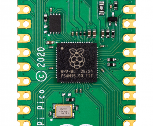
RP2040 has been in development since summer 2017. Chips are extremely complicated to design. In particular, the first chip you design requires you to design several fundamental components, which you can then reuse on future chips. The engineering effort was also diverted at some points in the project (for example to focus on the Raspberry Pi 4 launch).
Once the chip architecture is specified, the next stage of the project is the design and implementation, where hardware is described using a hardware description language such as Verilog. Verilog has been around since 1984 and, along with VHDL, has been used to design most chips in existence today. So what does Verilog look like, and how does it compare to writing software?
Suppose we have a C program that implements two wrapping counters:
void count_forever(void) {
    uint8_t i = 0;
    uint8_t j = 0;
    while (1) {
        i += 1;
        j += 1;
    }
}
This C program will execute sequentially line by line, and the processor won’t be able to do anything else (unless it is interrupted) while running this code. Let’s compare this with a Verilog implementation of the same counter:
module counter (
    input wire clk,
    input wire rst_n,
    output reg [7:0] i,
    output reg [7:0] j
);

always @ (posedge clk or negedge rst_n) begin
    if (~rst_n) begin
        // Counter is in reset so hold counter at 0
        i <= 8’d0;
        j <= 8’d0;
    end else begin
        i <= i + 8’d1;
        j <= j + 8’d1;
    end
end

endmodule
Verilog statements are executed in parallel on every clock cycle, so both i and j are updated at exactly the same time, whereas the C program increments i first, followed by j. Expanding on this idea, you can think of a chip as thousands of small Verilog modules like this, all executing in parallel.
A chip designer has several tools available to them to test the design. Testing/verification is the most important part of a chip design project: if a feature hasn’t been tested, then it probably doesn’t work. Two methods of testing used on RP2040 are simulators and FPGAs.
A simulator lets you simulate the entire chip design, and also some additional components. In RP2040’s case, we simulated RP2040 and an external flash chip, allowing us to run code from SPI flash in the simulator. That is the beauty of hardware design: you can design some hardware, then write some C code to test it, and then watch it all run cycle by cycle in the simulator.

The downside to simulators is that they are very slow. It can take several hours to simulate just one second of a chip. Simulation time can be reduced by testing blocks of hardware in isolation from the rest of the chip, but even then it is still slow. This is where FPGAs come in…
FPGAs (Field Programmable Gate Arrays) are chips that have reconfigurable logic, and can emulate the digital parts of a chip, allowing most of the logic in the chip to be tested.
FPGAs can’t emulate the analogue parts of a design, such as the resistors that are built into RP2040’s USB PHY. However, this can be approximated by using external hardware to provide analogue functionality. FPGAs often can’t run a design at full speed. In RP2040’s case, the FPGA was able to run at 48MHz (compared to 133MHz for the fully fledged chip). This is still fast enough to test everything we wanted and also develop software on.
FPGAs also have debug logic built into them. This allows the hardware designer to probe signals in the FPGA, and view them in a waveform viewer similar to the simulator above, although visibility is limited compared to the simulator.


The RP2040 bootrom was developed on FPGA, allowing us to test the USB boot mode, as well executing code from SPI flash. In the image above, the SD card slot on the FPGA is wired up to SPI flash using an SD card-shaped flash board designed by Luke Wren.

In parallel to Verilog development, the implementation team is busy making sure that the Verilog we write can actually be made into a real chip. Synthesis takes a Verilog description of the chip and converts the logic described into logic cells defined by your library choice. RP2040 is manufactured by TSMC, and we used their standard cell library.

Chip manufacturing isn’t perfect. So design for test (DFT) logic is inserted, allowing the logic in RP2040 to be tested during production to make sure there are no manufacturing defects (short or open circuit connections, for example). Chips that fail this production test are thrown away (this is a tiny percentage – the yield for RP2040 is particularly high due to the small die size).
After synthesis, the resulting netlist goes through a layout phase where the standard cells are physically placed and interconnect wires are routed. This is a synchronous design so clock trees are inserted, and timing is checked and fixed to make sure the design meets the clock speeds that we want. Once several design rules are checked, the layout can be exported to GDSII format, suitable for export to TSMC for manufacture.

(In reality, the process of synthesis, layout, and DFT insertion is extremely complicated and takes several months to get right, so the description here is just a highly abbreviated overview of the entire process.)
Once silicon wafers are manufactured at TSMC they need to be put into a package. After that, the first chips are sent to Pi Towers for bring-up!

A bring-up board typically has a socket (in the centre) so you can test several chips in a single board. It also separates each power supply on the chip, so you can limit the current on first power-up to check there are no shorts. You don’t want the magic smoke to escape!

Once the initial bring-up was done, RP2040 was put through its paces in the lab. Characterising behaviour, seeing how it performs at temperature and voltage extremes.

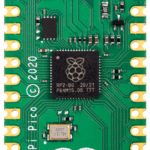
Once the initial batch of RP2040s are signed off we give the signal for mass production, ready for them to be put onto Pico boards that you have in your hands today.

A chip is useless without detailed documentation. While RP2040 was making its way to mass production, we spent several months writing the SDK and excellent documentation you have available to you today.

46 comments
Andrew Gale
Thank you – this was a very interesting article, it’s good to see a bit of the “behind the scenes” about the making of the RP2040. Is the packaging of dies into chips done by TSMC themselves or by a separate company?
Robert Sexton
There is a whole constellation of ‘Assembly and Test’ companies that take wafers and turn them into packaged, tested chips. Companies like TSMC also have their own in-house operations for this job.
solar3000
Very nice.
What a journey!
And thanks.
Stewart Watkiss
Thank you for giving details of how the Pico came about.
Well done for the documentation. It’s so nice being able to go to a single place where (almost) everything you need is documented without needing to search distributed datasheets.
Pranav Srinivas
Great article! I’m curious as to what kind of fundamental components you had to design when you mentioned “the first chip you design requires you to design several fundamental components”
Liam Fraser — post author
Each hardware block has a standard set of signals. A clock input, a reset input, signals to interface with GPIO pins, interrupt outputs, connections to the bus fabric, etc. All of the components that generate or interface with these standard signals had to be created, so that’s things like:
– Clock generators
– Reset controller
– GPIO controller
– Interrupt controller
– Bus Fabric
Hopefully a future blog post can dive into the detail of this some more!
Misel
Wow, the actual silicon is so tiny! :o
No wonder it’s called Pico :D
Jan
It’s pretty simple as today’s microcontrollers go and no onboard flash also save some space.
W. H. Heydt
Thanks much for the clear, and fairly concise, description of what it takes to develop a chip. This will be a useful article to point to the next time some remarks about an “easy” change to the RP2040…let alone a Pi SoC.
Anton
So interesting, thank you for posting it!
Richard collins
This is awesome, thanks for sharing. When is the documentary coming out? :D
Joking aside, if and when an RPi5 is created any chance of creating a documentary?
Please note, I don’t think we need another version of the RPi for a long time.
Jeff Greer
I hope all of you make the big bucks!
Simply amazing!
crumble
How have you managed to keep the wiring of “oh dear” in place? Was the desk off limits for children, pets and cleaning personal?
Neil Shepherd
My wife’s sewing room is very much “Oh dear”. It stays that way because I’m not allowed in!
scruss
Strong 8-bit energy from that DIL picture. Looks like you could drop it straight into a Beeb … and then see all of the magic smoke come out.
Lucas Morais
Nice article!
For simulation, have you given a shot to Verilator? I used it some time ago to model custom RISC-V instructions and it seemed a good open-source competitor to VCS.
James Young
Can we get more pics of the DIL RP2040 please?
andrum99
Presumably TSMC are shipping direct to Sony in Japan now?
Craig Van Degrift
Thank you for sharing this. This will surely inspire some future chip designers. RPi education in action.
spiralbrain
Fantastic Job!
Avijit Dhawan
Really Interesting Insights
Errol
Great article!
Love seeing a Saleae logic analyzer!
Tom
Why didn’t you go with Risv-V?
Anders
The DIL package appears to have all its pins shorted together. What’s the reason for that? Anti-static maybe?
Jan
No, that’s how those packages are made. You have sheet of metal which become grid of pins and then the pins are separated. At least this used to be true for such old style packages as CERDIP (ceramic dual in line package). These empty ones for prototyping your own chip seem to be pretty rare. Check out these https://www.chelseatech.com/packages.htm
Anders
I’ve worked with DIL packaged components for many years back when they were popular, and never saw one like that. The came packaged in long plastic static-treated tubes, with a stopper in the end (shaped like a U section) or they came in foiled lined cardboard boxes with their legs pushed into back anti-static foam.
The legs were always slightly splayed so they were run through a pair of rollers before being pushed into a PCB or DIL socket.
I guess the shorted legs are for these special prototypes.
Liam Fraser — post author
It turns out that this particular picture is of a package fail (there’s something to this effect written on the top in pencil), so they didn’t bother finishing the job and cutting off the end of the lead frame.
Anders
I’m tempted to be facetious and suggest that shorting all the pins is quite a big package fail :)
Thanks for the explanation.
CooliPi
Thanks for sharing your ‘behind the scenes’ story.
One question: What TSMC process variant have you used? There are Low Power (LP), General Purpose Superb (G) and low-power triple gate oxide (LPG) process options. Maybe even ULP, not counting flash nodes.
Liam Fraser — post author
We use the TSMC 40LP process.
JohnM
When I was involved in 4 phase MOS chip design in the 1970’s after the logic design was drawn – on paper the design was simulated on an midi computer. When that was correct the gates and interconnects were hand drawn onto large about 50″ square sheets of polyester drawing film that had a 0.1″ grid. When drawing the interconnects you had to be careful of the areas as if there was a large increase in capacitance between the input of the gate and the output the voltage would fall too far to operate. When complete the drawing was digitised using a hand digitiser and the resultant design file was checked using another computer programme. When this passed the masks were drawn on rubilith film using an X-Y plotter fitted with a cutter. The transparent parts then had to be peeled off by hand – if you made an error and lifted the wrong part there was no repair you had to cut another master and start again. How things have changed !! At least in those days we could see the layout of the finished chip with an optical microscope.
Wayne Keenan
awesome, thanks and great job.
Elfen
FPGAs can’t run above 48MHz? That depends on the FGPA one is using as there are many running in the GHz range for various applications including emulation of various systems. The statement should be used is the FPGA used to create the R-Pi Pico was limited in its speed to 48MHz.
Otherwise this was an interesting article though a bit generic and non-technical in terms. It introduces basic concepts to the laymen and beginner level DIYers, and shows the scope on what it entails to make such a a project possible from idea to drawing board to proof of concept and finally a final product.
Carl Mikkelsen
Elfen,
The maximum clock rate of the FPGA may have been higher, but the propagation time of the logic layers between the flops typically limits the maximum clock rate. Without looking at the detailed timing report for the placed and routed FPGA, it would be hard to know if there were higher speeds available.
Certainly many FPGAs have a max clock rate much higher than 48 MHz. With the right synthesis rules, any one of them could be constrained to be much slower.
Liam Fraser — post author
Carl is right. I said “In RP2040’s case, the FPGA was able to run at 48MHz “. A higher end FPGA would have been able to run the chip faster…
A small amount of logic in an FPGA can run at high speeds but if you try and fit a full chip in there then you have to slow it down to meet timing constraints. In particular, the system clock has to be slowed down because there is a lot of logic driven from that clock and the clock edges must arrive at the all of the logic at the same time.
Nick
Very interesting journey.
Ajahn Jhanarato
That’s a lot of equipment in those photos. Did you do much of that work from home?
Iuga Marian Silviu
Please, if I want to add microSDXC storage, what is the read and write speed. Can I use Linux kernel with ext4, btrfs or only FAT32 or exFAT ? I want to make a music player with the Raspberry Pi Pico – do you think it has the CPU speed to play FLAC files and use USB Sound card or a form of 16 bit DAC ?
Kevin
The Pico does not currently run Linux and no one has ported it yet. Until then it is likely possbile to do this using the built-in micropython that the Pico does run, though it will still require writing drivers for the SD card, filesystem, and audio hardware. If that sounds too hard difficult, go get a regular Pi Zero where you can have all those features right now, for just $1 more.
Adam Page
82K RP2040s in 11 boxes! What!?
Robert Sexton
This is a superb design. I like the CM0 IOPORT as a multiprocessor communications path and the all-too-rare 64-bit timebase timer. Thanks for keeping the VTOR. Did you use the ARM script-generated AHB matrix or roll your own? In your other comments you mention customizing the interrupt controller. Can you explain that a little? The data sheet suggests an NVIC.
Liam Fraser — post author
Thanks! We rolled our own Bus Fabric components. We didn’t modify ARM the interrupt controller but did build our own memory mapped register blocks that can generate interrupts. The “interrupt controller” in RP2040 is just some wiring. It creates a bus from each of the individual interrupts and then passes the bus to the NVIC in core0 and core1.
chepecarlos
How great is the article I did not know all the time they worked is the new processor, when do you think only the chip is available?
Alwyn Allan
Thanks for the details – most chip design happens in secret. Apart from the PIO state machines, I’m interested in the fractional clock dividers. Did you have to license Intel’s 2015 patent?
chipace
If you make a future version, an eFPGA would be a great peripheral. The one I am using is supported by Yosys and the open-source toolchains. People could actually build their own peripherals… what an amazing learning opportunity for children of all ages.
https://www.quicklogic.com/products/eos-s3/quickfeather-development-kit/
chipace
On my last project I put my analog models for ADC, comparators and autocal into the FGPA with the digital design. I had a separate SPI port load register mapped DAC values which drove the analog models. If you did analog modeling in the digital simulator, all of that can go in the FPGA also… it just needs to be converted from real types to 8 or 10bit DAC values. I finished all my python verification coding before silicon arrived. Hopefully you didn’t actually try to marry the FPGA to discrete analog circuits.
Comments are closed