Sustainable solutions with Raspberry Pi: how intrusive reflow soldering boosted our efficiency and cut our carbon footprint
We’ve reduced product returns by half, cut our manufacturing time by 15%, and eliminated 43 tonnes of CO₂ emissions per year by changing the way we solder connectors onto our computers.
In product design and manufacture, small changes often drive big differences in environmental impact, and at Raspberry Pi we’ve always made sure we have a thorough understanding of the processes used to manufacture our products so that we can spot ways to improve them. In the run-up to Raspberry Pi 5, we worked with our manufacturing partner Sony to implement a technique called intrusive reflow soldering, an adjustment that has improved product quality, reduced waste, and lowered our environmental impact.

Solving the through-hole bottleneck
Through-hole connectors have long been a sticking point in efficient production. They require robust solder joints made through the printed circuit board itself, meaning they can’t simply be handled by the standard processes used with SMT (Surface Mount Technology, aka pick-and-place) machines. Because of this, we have always endeavoured to minimise the number of through-hole parts, and this type of mounting is typically reserved for connectors. In the early days of Raspberry Pi, these parts were inserted by hand, and later by robotic placement. There then followed a wave soldering step — an additional process involving a molten solder bath which the boards pass through. This added time, cost, and complexity to our production line.
Thanks to our work with Sony, we have eliminated all of the through-hole–specific actions from our manufacturing processes. With intrusive reflow, we can now place through-hole connectors using the same pick-and-place machines we already use for surface-mount parts; this means there is no longer any need for bespoke robotics, or for an additional soldering stage. Over a series of trials, we perfected component placement, tweaked the solder paste stencil, refined the PCB layout, adapted the connector design, and adjusted the inspection process. We validated the results against our stringent quality control, successfully achieving all the standards that we set ourselves.
A new manufacturing standard for Raspberry Pi 5 and beyond
This became the production process that we have used on all Raspberry Pi 5 computers, and we’re working to roll it out to the manufacture of our earlier models too.

The change delivered a marked increase in product quality, with a massive 50% reduction in product returns. It also increased the speed at which products are manufactured by 15%. Work In Process (WIP) inventory was eliminated entirely, as there is no longer any break in the production line, all the way from bare boards coming into the factory to finished Raspberry Pi computers being packaged into boxes. And removing a set of machinery — the selective solder bath — from the production line reduced the CO₂ output of our production by 43 tonnes per year.
Smarter manufacturing, smaller footprint
Raspberry Pi’s move to intrusive reflow soldering shows how targeted changes in manufacturing can lead to significant improvements in sustainability. By cutting energy use, eliminating wasteful intermediate steps, and improving product quality, we’re reducing our environmental impact while making our production more efficient. It’s one of many ongoing efforts to manufacture more responsibly and more sustainably.


10 comments
Steven Blackburn
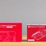
So the “intrusive” part is pushing connector legs through the solder paste? Is that why the connector legs look shorter on the RPI5 in the picture?
NB: The Wikipedia reflow article says “potentially reducing assembly costs.[clarification needed] “…. sounds like this blog entry could provide the clarification / citation.
Tom
Indeed. I’m not familar with the terms for “old” or “new” ways, and would have liked the article to explain each in detail and then contrast them against each other.
Seems this is a business/process presentation, rather than technical ? Could we get a follow up ?
Steve Drake
Could you explain what it means to use “intrusive reflow” what is it. I understand what reflow is how does the first word change the process.
Nick
“Through-hole connectors have long been a sticking point in efficient production.” :)) Very nice!
So… better product quality, with 50% less returns, 15% faster manufacturing, no more WIP, removed machines leading to a lot of energy use, less waste and significantly reduced CO₂. That’s really impressive for such small products. How does this translate into manufacturing costs? How will this impact the prices going forward?
And a side question: Should I complete my collection with a Raspberry Pi 2 B 1.2? I have the 1.1, but 1.2 was the first 64-bit Pi and kind of itches to have that too. :)
Anders
I had a collection of every version of Pi until the red and blue PCBs appeared and were unobtainable. So I gave up.
The GPIO connector pins are truly square pegs in round holes and the corner edges are in contact with through plating and desoldering is quite tricky.
Aaron Shaw
I have got both a red and blue PCB Pi ;-)
AndrewS
Raspberry Pi 3 Model B (with the BCM2837) was the first 64-bit Pi :-) See https://magazine.raspberrypi.com/issues/43
Raspberry Pi 2 Model B rev 1.2 wasn’t released until later, when the supply of BCM2836 chips (used on the original Raspberry Pi 2 Model B) ran out.
OldSkool
Wouldn’t have all the fallout if lead solder was used. RHOS is great for the environment, but making 15% more product because of higher RHOS defect rates is not good for the environment.
Matt
You cannot use lead solder in standard manufacturing, only for medical and military purpose…
Andrew Kirby
I think this the same as pin-in-paste? It might be new for RPi but I did my first board using this technique more than ten years ago… the trick was tuning the relative size of the PTH to the pin and then getting the solder paste stencil aperture right so the quantity of paste is correct to fill the void between the pin and the PTH over the thickness of the PCB. If the pin density is too high then there might not be enough surface area between the pins to get enough paste. It required the PCB designer to work very closely with a PCB assembler that has experience running this process. I am sure it is a lot easier now and more automated – it is more widespread practice and more connectors are available that are specifically designed for pin-in-paste processes. It was worth the effort as it saved me a lot of tooling costs by not having to selective solder the PTH parts. There wasn’t a massive difference in yield but the production costs were lower by only having to use one process.
Comments are closed